(YourDigitalWall Editorial):- Shenzhen, Guangdong May 31, 2026 (Issuewire.com) – Reliability in printed circuit board assembly often hinges on the integrity of the solder joint. While the industry has largely shifted toward lead-free alternatives, specific high-performance sectors continue to rely on traditional SnPb (Tin-Lead) compositions. Achieving perfection with these materials requires advanced atmospheric control. As a best leaded nitrogen vacuum reflow soldering solution provider, Venture Electronics integrates specialized thermal profiles with controlled environments to eliminate structural defects. This approach ensures that mission-critical electronics meet the rigorous demands of aerospace, medical, and defense applications where failure is not an option.
Why Does Leaded Soldering Remain a High-Reliability Choice in Vacuum Nitrogen Environments?
The transition to lead-free soldering was driven by environmental regulations, yet the physical properties of SnPb alloys offer distinct advantages for sensitive electronics. Leaded solder possesses a lower melting point than lead-free variants, typically around 183°C. This lower thermal threshold reduces the heat stress applied to delicate components during the reflow process. By combining this forgiving material with a nitrogen-purged vacuum environment, Venture Electronics achieves a level of stability that modern alternatives often struggle to match.
This hybrid methodology is not a regression in technology but a calculated engineering decision. For industries dealing with long-cycle products, such as military hardware or legacy aerospace systems, SnPb solder provides superior ductility and resistance to “tin whiskers.” These microscopic crystalline structures can cause short circuits in lead-free systems. When processed under vacuum, the internal pressure differentials remove volatile gases that would otherwise remain trapped. This results in a dense, uniform connection that is essential for thermal-sensitive devices like high-density Ball Grid Arrays (BGAs) and ceramic components.
How Do Vacuum and Nitrogen Synergize to Combat Voids and Oxidation?
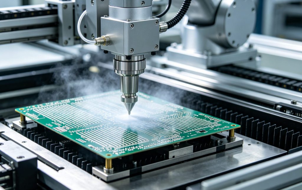
The science of a high-quality solder joint involves managing two primary enemies: gas entrapment and chemical degradation. Traditional reflow soldering often leaves behind “voids,” which are small pockets of air or flux vapors trapped within the solder ball. These voids reduce the effective contact area, leading to increased electrical resistance and potential mechanical failure under vibration. Venture Electronics utilizes specialized machinery to mitigate these issues through simultaneous atmospheric and pressure control.
During the molten phase of the reflow cycle, the vacuum stage introduces a controlled pressure drop. This physical mechanism forces flux vapors and air bubbles to the surface of the liquid solder, where they escape before solidification. This process significantly improves structural integrity, reducing void rates from a standard 20% down to a range of 1% to 5%. Such precision is critical for power electronics that require efficient heat dissipation through the solder interface.
Simultaneously, the introduction of a nitrogen atmosphere serves as a chemical shield. Oxygen is the primary catalyst for oxidation, which creates a non-conductive layer on copper pads and component leads. By maintaining an oxygen-depleted environment, nitrogen ensures that the leaded solder maintains maximum wettability. This allows the solder to flow smoothly and bond instantly, creating a robust metallurgical bridge with high shear strength.
Comparative Performance: Vacuum Leaded Soldering vs. Conventional Atmospheric Processes
The technical disparity between vacuum-based leaded soldering and traditional atmospheric soldering is most evident in the resulting performance data. Conventional processes often struggle with inconsistent heat distribution and atmospheric interference, leading to higher defect rates. In contrast, specialized vacuum systems used by Venture Electronics provide a highly controlled environment that produces repeatable, high-yield results.
While a standard atmospheric process typically results in a void rate between 15% and 20%, the vacuum nitrogen environment suppresses these defects to less than 5%. This reduction directly correlates to lower thermal resistance, which helps dissipate heat more effectively across the board. Furthermore, the vacuum process achieves a first-pass yield exceeding 99%, a significant improvement over the 92% average seen in traditional setups.
Beyond these metrics, the vacuum process expands the capabilities of traditional leaded soldering to modern substrates. It allows for the stable assembly of ultra-fine-pitch components (such as 0.35mm BGAs) on complex materials like aluminum-core boards, ceramic substrates, and rigid-flex circuits. These materials often present challenges due to their unique thermal expansion coefficients, but the lower temperatures of leaded solder combined with vacuum precision mitigate these risks.
Why Do Clients Invest in This Process Despite Higher Initial Costs?
From a Total Cost of Ownership (TCO) perspective, the decision to utilize nitrogen vacuum reflow soldering at Venture Electronics is an investment in long-term risk mitigation. While the individual board processing fee may be higher than standard reflow, the reduction in post-production costs is substantial. High-reliability sectors like the automotive and medical industries face astronomical costs if a field failure leads to a product recall.
By ensuring a near-zero defect rate at the assembly stage, manufacturers avoid the labor-intensive process of manual rework, which can often damage the PCB through repeated heat cycles. Furthermore, this process offers designers greater freedom. Engineers can specify high-density layouts and heat-sensitive components without compromising the structural viability of the board. The enhanced longevity provided by vacuum-soldered joints ensures that the device remains functional throughout its intended service life, even in harsh environments.
Quality Assurance from Parameter Freezing to Military-Standard Traceability
Maintaining consistency across multiple production batches requires a rigorous approach to quality control. Each project managed by Venture Electronics undergoes a “parameter freezing” phase where the specific thermal profile is locked. This involves precise temperature control within a margin of ±1°C. By stabilizing these variables, the process achieves identical results for every unit, whether it is a small prototype run or a high-volume production batch.
Traceability is the final pillar of this high-reliability solution. Adherence to standards such as MIL-STD-883 ensures that every step of the assembly is documented and verifiable. This includes comprehensive data logs from the component batches used to the final X-ray inspection reports that confirm void percentages. Such transparency provides the necessary documentation for defense and medical certifications, proving that the internal structure of every solder joint meets the highest global standards.
Venture Electronics continues to bridge the gap between traditional reliability and modern precision. By mastering the complexities of the nitrogen vacuum environment, the organization provides a stable foundation for the world’s most critical electronic systems.
Conclusion
By integrating the mechanical advantages of SnPb alloys with the precision of a nitrogen-purged vacuum environment, Venture Electronics effectively strengthens high-reliability manufacturing. This advanced process minimizes structural defects, ensures thermal stability, and provides a scalable solution for the world’s most demanding industries. As electronics continue to shrink in size but grow in complexity, the commitment to zero-defect quality through scientific process control remains the ultimate safeguard for mission-critical performance. From initial prototyping to full-scale production, this methodology ensures that every connection is built to endure the most extreme operating conditions.
To learn more about advanced soldering solutions, please visit: https://www.venture-mfg.com/

Media Contact
Venture Electronics Tech Ltd.
+86-0755-85296692
Building 36, Chentian Industrial Area Xixiang, Bao an District, Shenzhen, GuangDong, China
This article was originally published by IssueWire. Read the original article here.
![]()